Adjustable Voltage Output Multifunction 2A High Speed LDO Regulator
The XC6230 series are low on-resistance / low dropout voltage, highly precise, low noise, high PSRR, and large current High Speed LDO regulator IC. Internal circuitry includes a reference voltage supply, error amplifier, driver transistor, over-current protection circuit, in-rush current prevention circuit, reverse current protection circuit, thermal shutdown circuit, and phase compensation circuit. A built-in 0.17Ω low ON-resistance Pch driver transistor which can output up to a maximum output current 2.0A are also enclosed in a small surface-mount PKG, even in applications that input and output voltage difference is you use a very small state, it is possible to use in the space-saving. A low ESR ceramic capacitor can be used for the output capacitor (CL). Then, the output voltage is possible to set the output voltage value to 1.2V ~ 5.0V by connecting the external resistors to VOFB terminal. The over current protection circuit will operate when the output current reaches its current limit. The thermal shutdown circuit will operate when the junction temperature reaches its limit temperature. The current limit is possible to arbitrarily set in a range of external resistor in 0.3 ~ 2.5A to ILIM terminal. The inrush current prevention circuit perform the function of suppressing the variation of the VIN line and It is possible to suppress the current (inrush current), which is charged in the output capacitor (CL) during IC start rising (when the IC control in CE). In addition, the CE function enables the output to be turned off and the IC becomes a stand-by mode resulting in greatly reduced power consumption. When in standby mode, the output capacitor (CL) to be discharged at high speed it can be returned to the VSS level. The IC has further built-in reverse current prevention circuit, to prevent backflow current when the voltage state of more than input terminal (VIN) to the output terminal (VOUT).
Feature
| MaximumOutput Current | 2.0A |
| Current Limit Setting Range | 0.3A~2.5A |
| Dropout Voltage | 0.17V@IOUT=1.0A/VOUT_SET=3.3V |
| Operating Voltage Range | 1.7V~6.0V |
| Output VoltageAccuracy | 1.2V±1.0% |
| Output Voltage Range | 1.2V~5.0V |
| Quiescent Current | 45μA |
| Functions | Reverse Current Protection Inrush Current Prevention Output Voltage Adjustable CL High Speed Discharge Current Limit Adjustable |
| Protection Ciruit | Thermal Shutdown (Detect: 150℃, Release: 125℃ (TYP.)) Current Limit Short Protection |
| Capacitor | Ceramic Capacitor (4.7μF) |
| Operating Ambient Temperature | -40℃~+105℃ |
| Environmentally Friendly | EU RoHS compliant, Pb free |
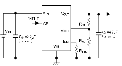
Typical Application Circuit
Quality Reports
Technical Document
Packages
XC6230 Series Part Numbers
| Part number | Sample | Type | Output Voltage | Output Voltage Accuracy | Packages | EDA | Online Store |
|---|---|---|---|---|---|---|---|
|
|
|
|
|
|
|
|
|
| XC6230A001ER-G | With CL AUTO-DISCHARGE | Adjustable Output Voltage(VOFB=1.2V) | ±1% | USP-6C |
|
||
| XC6230B001ER-G | Without CL AUTO-DISCHARGE | Adjustable Output Voltage(VOFB=1.2V) | ±1% | USP-6C |
|
||
| XC6230A001QR-G | With CL AUTO-DISCHARGE | Adjustable Output Voltage(VOFB=1.2V) | ±1% | SOP-8FD |
|
||
| XC6230B001QR-G | Without CL AUTO-DISCHARGE | Adjustable Output Voltage(VOFB=1.2V) | ±1% | SOP-8FD |
|
Inquiries About XC6230
Please wait for a while until the form is displaying.
If the form is not displaying, please contact us from inquiry form.