400mA Synchronous Step-Down DC/DC Converters
The XC9244 series is a group of synchronous-rectification type step-down DC/DC converters with a built-in 0.65ΩP-ch MOS driver transistor and 0.45Ω N-ch MOS switching transistor, designed to allow the use of ceramic capacitors. Output current of 400mA (MAX.) to be configured using only a coil and capacitor connected externally.
The output voltage can be set from 0.8V to 4.0V in increments of 0.05V (±2.0%). With an internal switching frequency of 1.2MHz, small external components can be used. USPN-6 package is suitable for the application which requires low profile and small-footprint.
When stand-by mode, due to stop all operation, quiescent current is reduced to 1μA or less. The integrated CL discharge function which enables the electric charge at the output capacitor CL to be discharged via the internal discharge switch located between the VOUT and VSS pins. The CL discharge function prevents malfunction on VOUT connecting application during stand-by mode.
The XC9244 series has a high speed soft-start as fast as 0.25ms in typical for quick turn-on. Current limiter circuit (Constant Current & Latching) is built-in for preventing from thermal destruction.
With UVLO (Under Voltage Lock Out) function, the internal P channel driver transistor is forced OFF when input voltage becomes 2.25V or lower.
Feature
| Driver Transistor | 0.65Ω P-ch Driver Transistor 0.45Ω N-ch Switching Transistor |
| Input Voltage Range | 2.3V~6.0V |
| Output Voltage Range | 0.8V~4.0V(0.05V increments) |
| High Efficiency | 90%(TYP.) |
| Output Current | 400mA |
| Oscillation Frequency | 1.2MHz(±15%) |
| Maximum Duty Cycle | 100% |
| Functions | Current Limit(Constant Current & Latching),CL High Speed Auto Discharge,Soft-Start |
| Capacitor | Low ESR Ceramic |
| Control Methods | PWM |
| Operating Ambient Temperature | -40℃~+85℃ |
| Environmentally Friendly | EU RoHS compliant, Pb free |
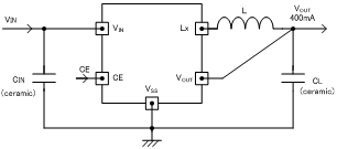
Typical Application Circuit
Quality Reports
Technical Document
Packages
| Package | Number of Pins | Pcs/Reel | Package Size(mm) |
|---|---|---|---|
| USPN-6 | 6 | 5,000 | 1.3 x 1.3 x 0.4 |
XC9244 Series Part Numbers
| Part number | Sample | Type | Output Voltage | Oscillation Frequency | Packages | EDA | Online Store |
|---|---|---|---|---|---|---|---|
|
|
|
|
|
|
|
|
|
| XC9244A08C7R-G | With CL Discharge, UVLO, Thermal Shutdown | 0.8V | 1.2MHz | USPN-6 |
|
||
| XC9244A09C7R-G | With CL Discharge, UVLO, Thermal Shutdown | 0.9V | 1.2MHz | USPN-6 |
|
||
| XC9244A0LC7R-G | With CL Discharge, UVLO, Thermal Shutdown | 0.85V | 1.2MHz | USPN-6 |
|
||
| XC9244A0MC7R-G | With CL Discharge, UVLO, Thermal Shutdown | 0.95V | 1.2MHz | USPN-6 |
|
||
| XC9244A10C7R-G | With CL Discharge, UVLO, Thermal Shutdown | 1.0V | 1.2MHz | USPN-6 |
|
||
| XC9244A11C7R-G | With CL Discharge, UVLO, Thermal Shutdown | 1.1V | 1.2MHz | USPN-6 |
|
||
| XC9244A12C7R-G | With CL Discharge, UVLO, Thermal Shutdown | 1.2V | 1.2MHz | USPN-6 |
|
||
| XC9244A13C7R-G | With CL Discharge, UVLO, Thermal Shutdown | 1.3V | 1.2MHz | USPN-6 |
|
||
| XC9244A14C7R-G | With CL Discharge, UVLO, Thermal Shutdown | 1.4V | 1.2MHz | USPN-6 |
|
||
| XC9244A15C7R-G | With CL Discharge, UVLO, Thermal Shutdown | 1.5V | 1.2MHz | USPN-6 |
|
||
| XC9244A16C7R-G | With CL Discharge, UVLO, Thermal Shutdown | 1.6V | 1.2MHz | USPN-6 |
|
||
| XC9244A17C7R-G | With CL Discharge, UVLO, Thermal Shutdown | 1.7V | 1.2MHz | USPN-6 |
|
||
| XC9244A18C7R-G | With CL Discharge, UVLO, Thermal Shutdown | 1.8V | 1.2MHz | USPN-6 |
|
||
| XC9244A19C7R-G | With CL Discharge, UVLO, Thermal Shutdown | 1.9V | 1.2MHz | USPN-6 |
|
||
| XC9244A1AC7R-G | With CL Discharge, UVLO, Thermal Shutdown | 1.05V | 1.2MHz | USPN-6 |
|
||
| XC9244A1BC7R-G | With CL Discharge, UVLO, Thermal Shutdown | 1.15V | 1.2MHz | USPN-6 |
|
||
| XC9244A1CC7R-G | With CL Discharge, UVLO, Thermal Shutdown | 1.25V | 1.2MHz | USPN-6 |
|
||
| XC9244A1DC7R-G | With CL Discharge, UVLO, Thermal Shutdown | 1.35V | 1.2MHz | USPN-6 |
|
||
| XC9244A1EC7R-G | With CL Discharge, UVLO, Thermal Shutdown | 1.45V | 1.2MHz | USPN-6 |
|
||
| XC9244A1FC7R-G | With CL Discharge, UVLO, Thermal Shutdown | 1.55V | 1.2MHz | USPN-6 |
|
||
| XC9244A1HC7R-G | With CL Discharge, UVLO, Thermal Shutdown | 1.65V | 1.2MHz | USPN-6 |
|
||
| XC9244A1KC7R-G | With CL Discharge, UVLO, Thermal Shutdown | 1.75V | 1.2MHz | USPN-6 |
|
||
| XC9244A1LC7R-G | With CL Discharge, UVLO, Thermal Shutdown | 1.85V | 1.2MHz | USPN-6 |
|
||
| XC9244A1MC7R-G | With CL Discharge, UVLO, Thermal Shutdown | 1.95V | 1.2MHz | USPN-6 |
|
||
| XC9244A20C7R-G | With CL Discharge, UVLO, Thermal Shutdown | 2.0V | 1.2MHz | USPN-6 |
|
||
| XC9244A21C7R-G | With CL Discharge, UVLO, Thermal Shutdown | 2.1V | 1.2MHz | USPN-6 |
|
||
| XC9244A22C7R-G | With CL Discharge, UVLO, Thermal Shutdown | 2.2V | 1.2MHz | USPN-6 |
|
||
| XC9244A23C7R-G | With CL Discharge, UVLO, Thermal Shutdown | 2.3V | 1.2MHz | USPN-6 |
|
||
| XC9244A24C7R-G | With CL Discharge, UVLO, Thermal Shutdown | 2.4V | 1.2MHz | USPN-6 |
|
||
| XC9244A25C7R-G | With CL Discharge, UVLO, Thermal Shutdown | 2.5V | 1.2MHz | USPN-6 |
|
||
| XC9244A26C7R-G | With CL Discharge, UVLO, Thermal Shutdown | 2.6V | 1.2MHz | USPN-6 |
|
||
| XC9244A27C7R-G | With CL Discharge, UVLO, Thermal Shutdown | 2.7V | 1.2MHz | USPN-6 |
|
||
| XC9244A28C7R-G | With CL Discharge, UVLO, Thermal Shutdown | 2.8V | 1.2MHz | USPN-6 |
|
||
| XC9244A29C7R-G | With CL Discharge, UVLO, Thermal Shutdown | 2.9V | 1.2MHz | USPN-6 |
|
||
| XC9244A2AC7R-G | With CL Discharge, UVLO, Thermal Shutdown | 2.05V | 1.2MHz | USPN-6 |
|
||
| XC9244A2BC7R-G | With CL Discharge, UVLO, Thermal Shutdown | 2.15V | 1.2MHz | USPN-6 |
|
||
| XC9244A2CC7R-G | With CL Discharge, UVLO, Thermal Shutdown | 2.25V | 1.2MHz | USPN-6 |
|
||
| XC9244A2DC7R-G | With CL Discharge, UVLO, Thermal Shutdown | 2.35V | 1.2MHz | USPN-6 |
|
||
| XC9244A2EC7R-G | With CL Discharge, UVLO, Thermal Shutdown | 2.45V | 1.2MHz | USPN-6 |
|
||
| XC9244A2FC7R-G | With CL Discharge, UVLO, Thermal Shutdown | 2.55V | 1.2MHz | USPN-6 |
|
||
| XC9244A2HC7R-G | With CL Discharge, UVLO, Thermal Shutdown | 2.65V | 1.2MHz | USPN-6 |
|
||
| XC9244A2KC7R-G | With CL Discharge, UVLO, Thermal Shutdown | 2.75V | 1.2MHz | USPN-6 |
|
||
| XC9244A2LC7R-G | With CL Discharge, UVLO, Thermal Shutdown | 2.85V | 1.2MHz | USPN-6 |
|
||
| XC9244A2MC7R-G | With CL Discharge, UVLO, Thermal Shutdown | 2.95V | 1.2MHz | USPN-6 |
|
||
| XC9244A30C7R-G | With CL Discharge, UVLO, Thermal Shutdown | 3.0V | 1.2MHz | USPN-6 |
|
||
| XC9244A31C7R-G | With CL Discharge, UVLO, Thermal Shutdown | 3.1V | 1.2MHz | USPN-6 |
|
||
| XC9244A32C7R-G | With CL Discharge, UVLO, Thermal Shutdown | 3.2V | 1.2MHz | USPN-6 |
|
||
| XC9244A33C7R-G | With CL Discharge, UVLO, Thermal Shutdown | 3.3V | 1.2MHz | USPN-6 |
|
||
| XC9244A34C7R-G | With CL Discharge, UVLO, Thermal Shutdown | 3.4V | 1.2MHz | USPN-6 |
|
||
| XC9244A35C7R-G | With CL Discharge, UVLO, Thermal Shutdown | 3.5V | 1.2MHz | USPN-6 |
|
||
| XC9244A36C7R-G | With CL Discharge, UVLO, Thermal Shutdown | 3.6V | 1.2MHz | USPN-6 |
|
||
| XC9244A37C7R-G | With CL Discharge, UVLO, Thermal Shutdown | 3.7V | 1.2MHz | USPN-6 |
|
||
| XC9244A38C7R-G | With CL Discharge, UVLO, Thermal Shutdown | 3.8V | 1.2MHz | USPN-6 |
|
||
| XC9244A39C7R-G | With CL Discharge, UVLO, Thermal Shutdown | 3.9V | 1.2MHz | USPN-6 |
|
||
| XC9244A3AC7R-G | With CL Discharge, UVLO, Thermal Shutdown | 3.05V | 1.2MHz | USPN-6 |
|
||
| XC9244A3BC7R-G | With CL Discharge, UVLO, Thermal Shutdown | 3.15V | 1.2MHz | USPN-6 |
|
||
| XC9244A3CC7R-G | With CL Discharge, UVLO, Thermal Shutdown | 3.25V | 1.2MHz | USPN-6 |
|
||
| XC9244A3DC7R-G | With CL Discharge, UVLO, Thermal Shutdown | 3.35V | 1.2MHz | USPN-6 |
|
||
| XC9244A3EC7R-G | With CL Discharge, UVLO, Thermal Shutdown | 3.45V | 1.2MHz | USPN-6 |
|
||
| XC9244A3FC7R-G | With CL Discharge, UVLO, Thermal Shutdown | 3.55V | 1.2MHz | USPN-6 |
|
||
| XC9244A3HC7R-G | With CL Discharge, UVLO, Thermal Shutdown | 3.65V | 1.2MHz | USPN-6 |
|
||
| XC9244A3KC7R-G | With CL Discharge, UVLO, Thermal Shutdown | 3.75V | 1.2MHz | USPN-6 |
|
||
| XC9244A3LC7R-G | With CL Discharge, UVLO, Thermal Shutdown | 3.85V | 1.2MHz | USPN-6 |
|
||
| XC9244A3MC7R-G | With CL Discharge, UVLO, Thermal Shutdown | 3.95V | 1.2MHz | USPN-6 |
|
||
| XC9244A40C7R-G | With CL Discharge, UVLO, Thermal Shutdown | 4.0V | 1.2MHz | USPN-6 |
|
Inquiries About XC9244
Please wait for a while until the form is displaying.
If the form is not displaying, please contact us from inquiry form.