Peripheral Parts Selection/PCB Design/Thermal Design/Simulation
- Where can I download 3D models / step files for 3D CAD?
-
TOREX is affiliated with a parts library provider, SamacSys and is able to provide libraries compatible with various EDA tools.
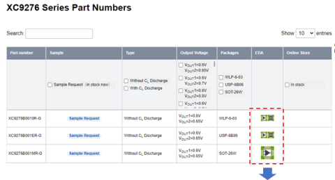
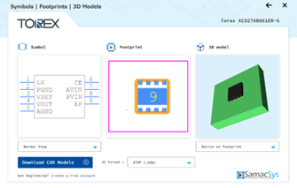
When you download libraries, you can download 3D models and step files for 3D CAD from each product page.If a library is prepared, you can immediately download the library by just creating SamacSys account. If no library is prepared, you can request creation of model library.Usually, a library can be provided in approximately 24 to 48 hours after request for creation.
“Product page” → “PCB Symbol, Footprint & 3D Model”
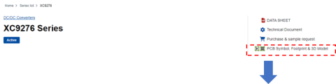
With library 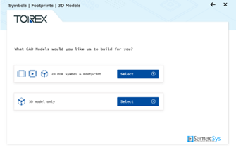
Without library (Request screen for library creation) - Where can I download the parts library for PCB design (footprint, symbol)?
-
TOREX is affiliated with a parts library provider, SamacSys and provides libraries compatible with various EDA tools.
When you download libraries, you can download parts library for PCB design (footprint, symbol) from each product page.
If a library is prepared, you can immediately download the library by just creating SamacSys account.
If no library is prepared, you can request creation of model library.
Usually, a library can be provided in approximately 24 to 48 hours after request for creation."Product page" → "PCB Symbol, Footprint & 3D Model"
With library Without library (Request screen for library creation)
Fundamentals of Electrical/Electronic Circuit
- What are High voltage, Low voltage?
-
High voltage is when the input voltage is voltage that is recognized as being high when it is above this value.
Conversely, low voltage is when the input voltage is voltage that is recognized as being low when it is below this value.Let’s look at the high voltage and low voltage of the voltage regulator’s CE terminal to see how this is specified for an actual product.
DC/DC converter (XC9236): Electrical characteristics
PARAMETER SYMBOL CONDITIONS MIN. TYP. MAX. UNIT CIRCUIT CE "H" Voltage VCEH VOUT=0V, Applied voltage to VCE, Voltage changes Lx to “H” level 0.65 - 6.0 V ③ CE "L" Voltage VCEL VOUT=0V, Applied voltage to VCE, Voltage changes Lx to “L” level VSS - 0.25 V ③ For the above product:
CE function high voltage : Always recognized as high when 0.65V to 6.0V
CE function low voltage : Always recognized as low when VSS (0V) to 0.25V
To put it another way, this shows that it is not possible to tell if the CE function is high or low when the applied voltage is between 0.25V to 0.65V.
To ensure the high/low state, it is important to design the product to ensure the input voltage is within the high voltage/low voltage range.
- What are power conversion efficiency and power supply efficiency? How is the efficiency measured?
-
Power conversion efficiency and power supply efficiency indicate the ratio of output power to input power.
Efficiency [%] = (output power / input power) x 100
Loss = output power - input powerIf the efficiency is high, the power to obtain the output power can be reduced and the conversion loss also becomes small. That is to say, if the efficiency is high, the power consumption is low, loss is low, and amount of heat generation is small.
When calculating a single power supply efficiency of DC/DC converter or voltage regulator, etc., following calculation is available.
Efficiency [%] = (output power / input power) x 100
= (output voltage x output current) / (input voltage x input current) x 100How to measure the efficiency
The efficiency under each condition can be obtained by correctly measuring output voltage, output current, input voltage, and input current using stabilized power supply, multimeter, electronic load / resistance load, etc.
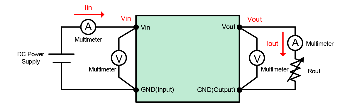
To measure the current, it is necessary to insert a multimeter into input / output line. As multimeter causes voltage drop, correct measurement of input voltage / output voltage near IC is required for correct calculation of efficiency.
In addition, using voltage setting value of stabilized power supply or output voltage setting value of DC/DC converter / voltage regulator for calculation of efficiency causes wrong calculation of efficiency.
- What are pull-up and pull-down resistances? What is an unstable state?
-
Pull-up resistance and pull-down resistance are resistances that stop the unstable state of the input and output terminals.
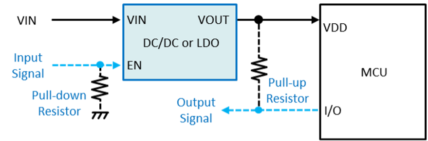
The input terminal becomes unstable state when the terminal is open and the connection destination is high impedance.
If there is a pull-up resistance and pull-down resistance, the state of the input and output terminals can be made to be High or Low even if the terminal is open.
For the output terminal, when the IC is not within the range of normal operation, such as during low input voltage, the state becomes unstable such that it is not possible to tell whether the output voltage will be High or Low.
When the output signal is unstable, the devices downstream from that input signal will enter an unintended state, which will cause an increase in the quiescent current or a malfunction. For this reason, the product must be designed to certainly be High or Low to prevent the devices from unintentional operation.
Further, in the unstable state, what the voltage will be cannot be known due to the IC’s leak current or the external noise, etc.
For this reason, the state may differ even in the same circuit due to the surrounding environment and variance in the IC or components.
- What is a load current?
-
The load current is the current that is supplied to the output capacity that is connected to a downstream device or output line that is a load.
When viewed from the power supply IC, the load device is connected to the output side of the power supply IC, so this is a load current to the power supply IC.
Rather than a load current, this can also be called an output current (IOUT), etc.
- What is a threshold?
-
A threshold is the voltage at the boundary between “0 (Low)” and “1 (High)” in mainly digital circuits.
When a voltage higher than the threshold is applied to the IC input terminal, it is recognized as being “High.” When the voltage is lower than the threshold, it is recognized as being “Low.”
When a voltage close to the threshold value is applied, the state becomes unstable without it being known whether it will be “High” or “Low” due to IC variance, fluctuation in the applied voltage, etc., which could cause the IC to malfunction.
For this reason, the “High voltage” and “Low voltage” specifications for the IC input terminal are generally set to voltages that are a distance from the threshold value.
Product Training (Basic/Operation Theory/Evaluation Method)
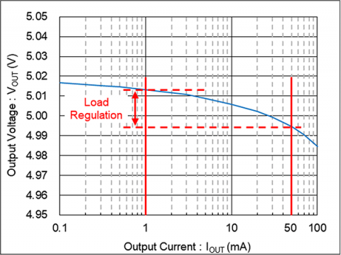
- What are the characteristics of load stability and load regulation?
-
Load regulation is the characteristic that shows how much the output voltage changes before and after the output current is increased.
This is expressed by the _mV change in the output voltage when the output current is changed from _mA to _mA. As the output current increases, the output voltage decreases, so generally the electrical characteristics of these products are fixed.
In the example below, we can see the voltage decreases by 50 mV when the current is changed from 1 mA to 50 mA.
Voltage regulator (XC6216 Vout=5.0V)
PARAMETER SYMBOL CONDITIONS MIN. TYP. MAX. UNITS CIRCUIT Load Regulation △Vout 1mA≦IOUT≦50mA, VCE=VIN - 50 90 mV ① Voltage regulator (XC6216 Vout=5.0V): Output voltage vs. output current characteristic
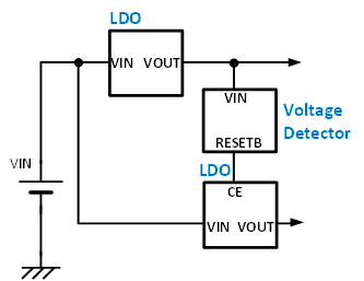
- What is the release delay of a voltage detector?
-
Release delay function
The release delay function of voltage detector is a function that does not output a release signal immediately after the monitoring voltage reaches the release voltage, but outputs it after a certain period of time has passed.
This delay time is called release delay time. There are products for which release delay time is set in IC and products for which release delay time can be externally adjusted using an external capacitor.
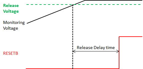
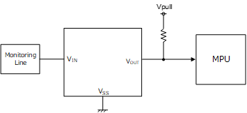
Products for which delay time is internally set 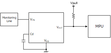
Products for which delay time can be externally adjusted Why is the release delay time required?
Immediately after startup of power supply, the voltage may not be stabilized due to ringing, etc.
In such a case, if you use a voltage detector without release delay function, the output of voltage detector may repeat "H" and "L" in the area where the power supply voltage fluctuates. This repetition of "H" and "L" may lead to malfunction of following MCU.
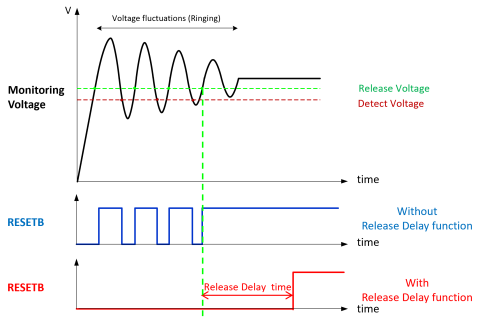
In order to prevent such malfunction, the release delay function (release delay time) is required so that a release signal is output after the power supply voltage gets stabilized.
The followings are typical example of power supply line instability other than startup of power supply.
- When turning ON/OFF a mechanical switch (chattering of mechanical switches)
- When the impedance of power supply line is large / wiring is long
- Chattering when batteries are inserted or mounted
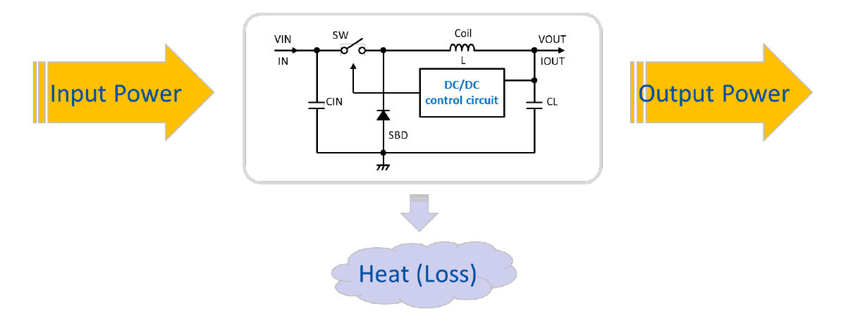
- Why are DC/DC converters more efficient than voltage regulators?
-
A DC/DC converter is more efficient than a voltage regulator because the method for controlling the output voltage is different.
A voltage regulator controls the output voltage by adjusting the driver FET’s ON resistance. In other words, the dropout voltage, which is the difference between the input voltage and the output voltage, in the driver FET decreases the voltage in the IC.
This driver FET voltage decrease results in loss, so the ideal voltage regulator efficiency is “VOUT/VIN x 100”.
On the other hand, a DC/DC converter controls the output voltage by adjusting the ON/OFF time of the driver FET.
The ON resistance is low while the driver FET is ON, so the conduction loss is small while current is flowing in the ON resistor and driver FET. Switching loss and other losses in addition to the conduction loss also occur, but even when including these the loss is less than that of the conduction loss, which makes a DC/DC converter more efficient than a voltage regulator.
The above is a general explanation, and the efficiency will differ depending on the power supply specifications, IC quiescent current, or the ON resistance of the DC/DC converter.
There might be times when the voltage regulator is more efficient depending on these conditions, so it is important to select the optimum product based on the usage conditions.
- How to calculate the pull-up/pull-down resistance value inside the IC?
-
Here introduces how to calculate pull-up resistance / pull-down resistance when they are not specified for an IC that has built-in pull-up resistance / pull-down resistance.
Step1:Confirmation of block diagram
Before calculating pull-up resistance/pull-down resistance, it is important to confirm the block diagram.
This is because that pull-up/pull-down may not be executed by resistance, but the pull-up/pull-down may be executed by a constant current element.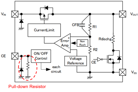
Voltage regulator XC6228: pull-down by resistance 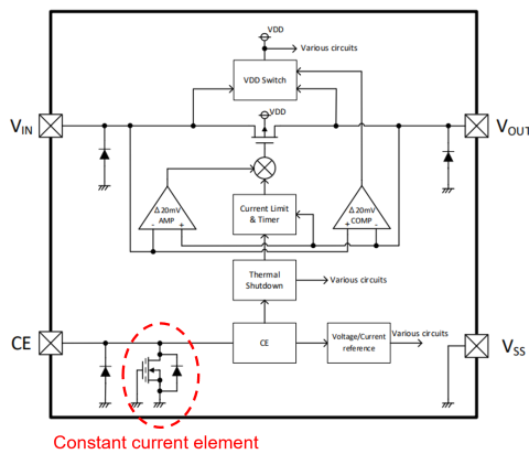
Load SW XC8111: pull-down by constant current element If pull-up / pull-down is executed by constant current element, the current does not vary depending on the applied voltage and the current becomes constant unlike resistance. Let's refer to the terminal current shown on the data sheet.
Step2:Calculation of resistance value
If the block diagram shows that pull-up / pull-down is executed by resistance, check the terminal current on the data sheet. Here explains it referencing the voltage regulator XC6228 that has CE terminal equipped with built-in pull-down resistance.
Voltage regulator XC6228 block diagram As XC6228 is equipped with pull-down resistance, check the terminal current at CE "H" where the current flows into pull-down resistance.
XC6228 CE "H" terminal current
PARAMETER SYMBOL CONDITIONS MIN. TYP. MAX. UNITS CE "H" Current ICEH VCE=VIN=5.5V 3.0 5.5 9.0 μA Here, check the measurement conditions (CONDITIONS) specifying CE "H" Current.
" VCE=VIN=5.5V " described for CONDITIONS means that "H" Current when CE = 5.5 V is applied is specified. The voltage to which CE is applied to the pull-down resistance. Thus, if 5.5 V is applied to pull-down resistance, CE "H" Current flows.
If you understand this far, you can calculate the pull-down resistance value using Ohm's law.
The following formula is calculated by Ohm's law "R = V / I".CE applied voltage = CE “H” Current x “pull-down resistance”
Using the above formula, the pull-down resistor can be calculated as follows.
Pull-down resistance MIN = 5.5V / CE “H” Current MAX = 611kΩ
Pull-down resistance TYP = 5.5V / CE “H” Current TYP = 1000kΩ
Pull-down resistance MAX = 5.5V / CE “H” Current MIN = 1833kΩ
Here calculated the resistance value referencing the pull-down resistance, however, you can also calculate the pull-up resistance in the same way.
- Is there a problem if the hysteresis width of the voltage detector, detection voltage, UVLO, etc. is small?
-
Here explains what kind of phenomenon occurs referencing the case when the hysteresis width of detect voltage / release voltage of voltage detector is small.
If the hysteresis width is small
Assume a circuit that monitors battery voltage with a voltage detector for which MCU is connected to a battery with large internal impedance such as coin battery.
In such a case, phenomenon in which detection and release of voltage detector are repeated may occur.Here explains how such a situation actually occurs in chronological order from steps 1 to 6.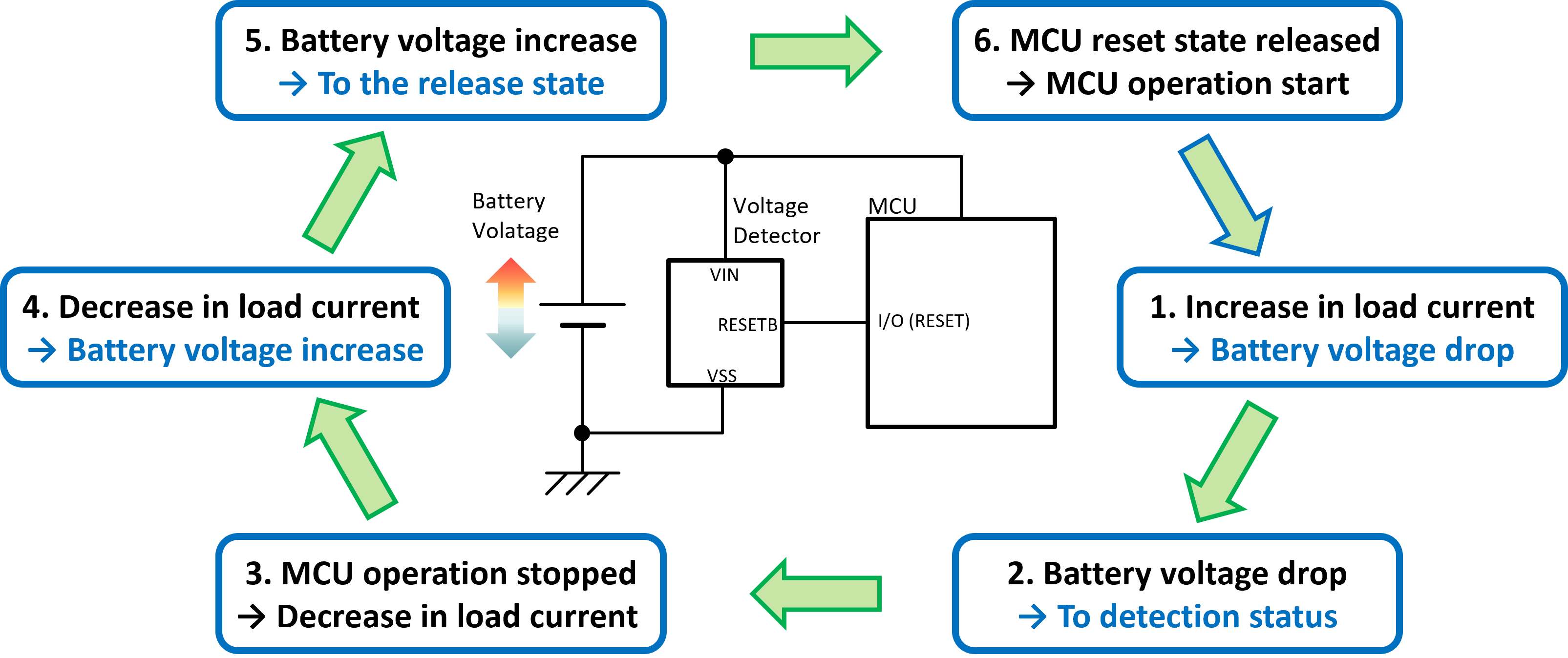
1. If the battery current increases, the battery voltage decreases due to the battery current and the battery's internal impedance.
2. If the battery voltage decreases, the voltage detector enters the detection status.If the voltage detector enters the detection status, a reset signal will be sent to MCU to stop the operation of MCU.
3. If MCU stops the operation, the load current decreases.
4. If the load current decreases, the voltage drop due to battery current and battery's internal impedance gets eliminated and the battery voltage increases.
5. If the battery voltage increases, the voltage detector enters release status and operates MCU.
6. The load current (battery current) of MCU increases.
* Steps 1 to 6 are repeated, detection and release statuses of voltage detector will be repeated.To prevent detection and release of voltage detector
The phenomenon in which detection and release of voltage detector are repeated is caused by fluctuation of battery voltage due to load current. If the fluctuation range of battery voltage is larger than the hysteresis width of voltage detector, detection and release statuses of voltage detector are repeated.
This time, the voltage fluctuation due to battery's internal impedance was taken as an example. However, even in the resistance components of fuses and filter circuits, the voltage fluctuation of a line monitored by voltage detector occurs and it causes repetition of detection and release statuses of voltage detector.
The followings are available as general measures.
・ Setting the hysteresis width larger than voltage fluctuation range of battery voltage (monitoring line)
・ Changing the battery with a battery whose internal impedance is small / changing the fuse filter with a fuse filter whose DCR is smallFor other than voltage detector
A case example was explained as shown above referencing the voltage detector. However, a similar phenomenon occurs in devices other than voltage detector.
The followings are case examples in which hysteresis width was small and detection and release statuses were continued.
(a) When the hysteresis width of UVLO detect voltage and release voltage of voltage regulator or DC/DC converter equipped with UVLO function is small
(b) When the hysteresis of CE/EN "L" voltage and "H" voltage of voltage regulator or DC/DC converter equipped with CE/EN function is smallIn addition to case examples shown above, a case example in which abnormal status and startup / steady status are repeated occurs if overcurrent protection, overheat protection, or low voltage protection, etc. of IC or circuit operates.
It is important to comprehend the operation of ICs and parts in the entire circuit instead of just seeing a single IC or part to design a circuit. - Please tell me about the current limit method of the voltage regulator
-
See here for the method of current limit characteristics (VOUT vs IOUT) of voltage regulators.
- What are differences among load disconnection, bypass, and Vout OR of step-up DC/DC
-
With a general voltage regulator and a step-down DC/DC, the output voltage when IC is in standby status (when the operation is stopped) decreases to 0V.
With a step-up DC/DC converter, the output voltage when IC is in standby status (when the operation is stopped) varies depending on the IC. Step-up DC/DC converters, types, and functions can be roughly classified into four types.
1. Non-synchronous type
This is a general step-up DC/DC converter that uses diode.
As a diode is used, input side and output side cannot be disconnected in standby status and electrical connection is executed via diode.A step-up DC/DC converter on which a driver is mounted operates in the same way as non-synchronous type step-up DC/DC converter when parasitic diode of a driver on High Side is not controlled.
2. Load disconnection function (product equipped with built-in Low Side/High Side driver FET)
The driver FET on High Side is controlled so that the output voltage becomes 0V in standby status.
(Driver FET: OFF, parasitic diode: anode Vout, cathode Lx)The load disconnection function disconnects input side and output side in standby status.
With this function, the output voltage decreases to 0V to prevent malfunction of system and reduce the power consumption.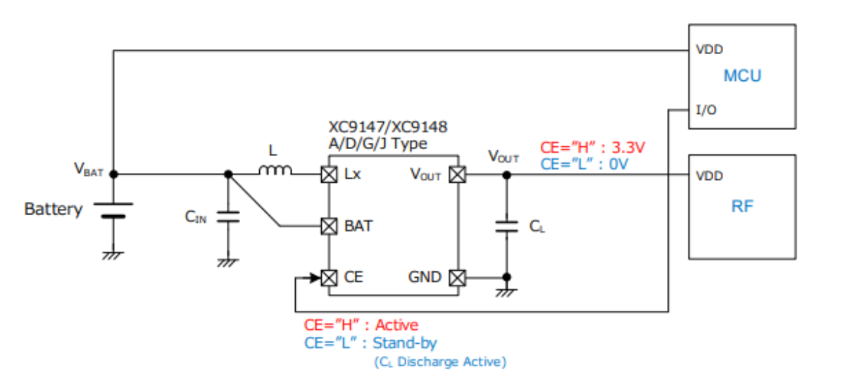
3. Bypass function (product equipped with built-in Low Side/High Side driver FET)
The driver FET on High Side is turned ON so that output side can be electrically connected with input in standby status.
With the bypass function, the input voltage can be passed through to the output side in standby status.
Utilizing this function can supply the battery voltage to the system side by setting it to standby status when MCU is in sleep status, for example. For RF that requires high supply voltage or at high-speed operation, voltage such as 3.3 V can be supplied to the system side by implementing the step-up operation.
The power consumption of whole system can be reduced by this voltage switching.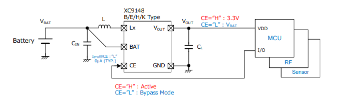
4. Vout "OR" type (product equipped with built-in Low Side/High Side driver FET)
This is Vout "OR" type enabling OR connection that applies external power supply to the output side.
With Vout "OR" type, input voltage and output voltage are monitored for both of step-up operation and standby status.It determines which is higher, input voltage or output voltage, and controls the polarity of parasitic diode of High Side driver FET to prevent backward flow via parasitic diode.
- What are High Active and Low Active?
-
A function that operates when the input signal is High is said to operate at High Active or Active High.
Conversely, a function that operates when the input signal is Low is said to operate at Low Active or Active Low.Load SW (XC8107): CE logical table
Active High
Logic CE Level Status Active High H Active L Stand-by OPEN Undefined State Active Low
Logic CE Level Status Active Low H Stand-by L Active OPEN Undefined State - What are Nch open drain output and CMOS output?
-
Nch open drain output and CMOS output show the type of output configuration of the output terminal.
Nch open drain output
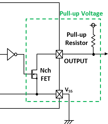
CMOS output
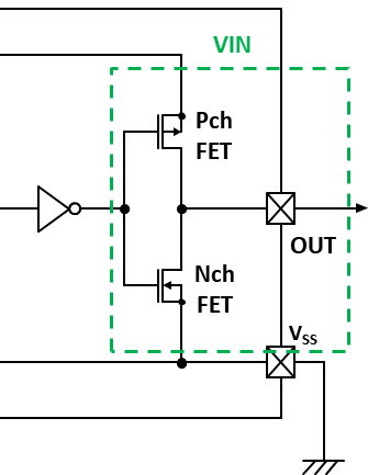
Nch open drain output: output voltage
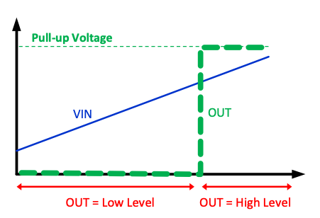
CMOS output: output voltage
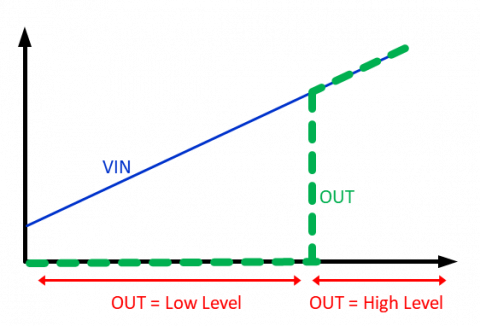
The Nch open drain output is only input by the Nch FET between the output terminal and the ground terminal.
FET is only input to the ground side, so pull-up resistance and pull-up voltage needs to be provided externally. Providing pull-up voltage to match the output destination microcomputer, etc., makes it possible to change the level of the output voltage to match the output destination device.In the CMOS output, a CMOS inverter is built into the output terminal.
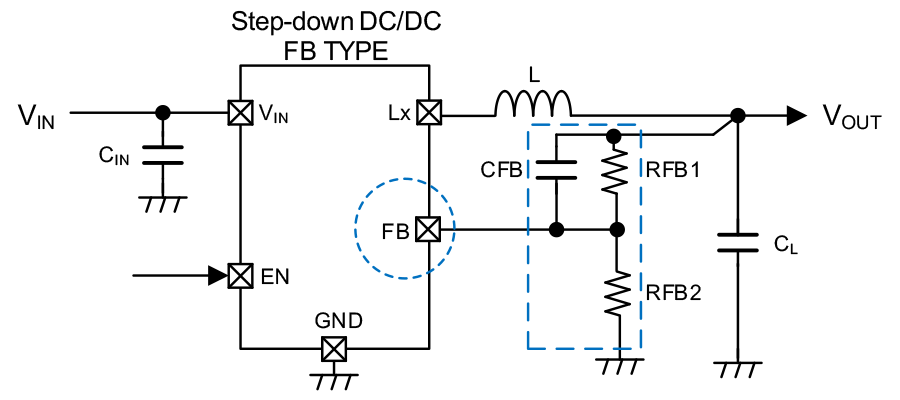
Unlike the Nch open drain output, there is no need to provide a pull-up resistance or pull-up voltage. For this reason, a quiescent current that flows in the pull-up resistance does not exist in the CMOS output, so this is optimum for low consumption applications.Nch Open Drain Output CMOS Output Output voltage High voltage Pull-up voltage VIN Low voltage 0V 0V Quiescent current Current consumption when output “L” 0μA Power-up speed Dependent on pull-up resistance Fast Parallel connection Multiple Nch open drains can be connected in parallel Not possible - What are output voltage fixed products (Vout products) and output voltage externally adjusted products (FB products)?
-
Output voltage fixed products (Vout products) and output voltage externally adjusted products (FB products) show the output voltage setting method for DC/DC and voltage regulators.
An output voltage fixed product (Vout product) is a product in which the output voltage is fixed inside the IC, and an output voltage externally adjusted product (FB product) is a product that can adjust the output voltage using an externally connected resistance, etc.
(a) Output voltage fixed products (Vout products)
An output voltage fixed product has a high-accuracy feedback resistance for adjusting the output voltage built into the IC. An externally connected resistance to adjust the output voltage is not required, making miniaturization and component reduction possible.
In addition, since the feedback resistance is built into the IC, the product is resistant to external noise and a higher feedback resistance value than with output voltage externally adjusted products can be used.
This makes it possible to hold down the quiescent current consumed by the feedback resistance, making it optimal for low consumption applications.
(b) Output voltage externally adjusted products (FB products)
An output voltage externally adjusted product requires the feedback resistance for adjusting the output voltage to be external to the IC. Since the output voltage can be changed by just changing the externally connected resistance, this type of product can be used to build multiple power supply lines using the same IC, which is advantageous for components control and inventory control.
A disadvantage is that an externally connected feedback resistance and a phase compensation capacitor are required, so there is a greater number of components compared to an output voltage fixed product.
In addition, since there is a feedback resistance external to the IC, the product is more easily affected by external noise, and if the feedback resistance value is too high, the IC could malfunction, so caution is required.
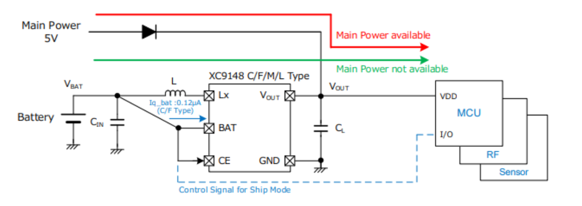
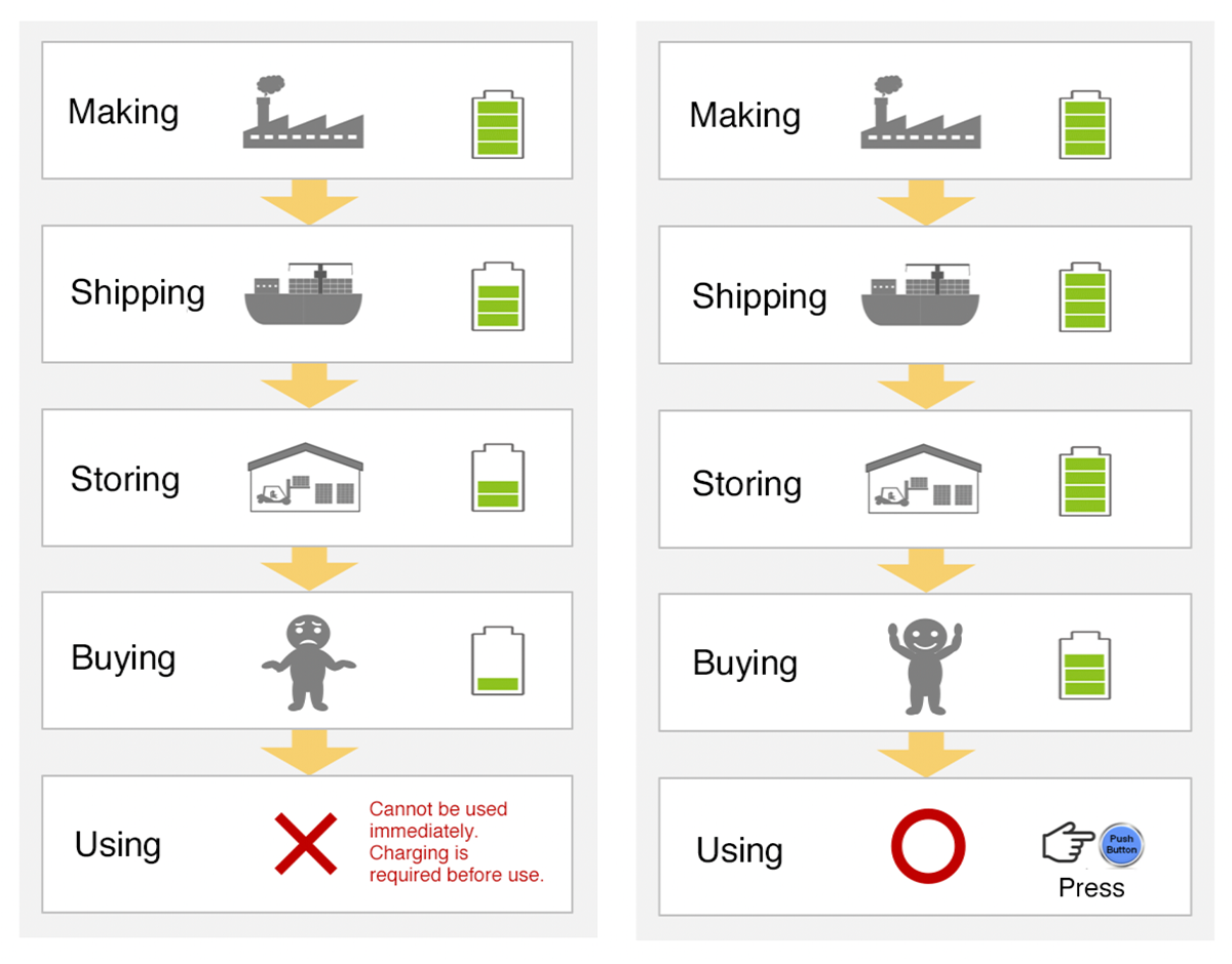
- What are ship function and shipping mode?
-
What is ship function?
The ship function is a function to prevent the remaining battery power from decreasing during long-term storage after the shipment of product. The ship function is sometimes called shipping mode, etc.
The electronic devices that have no ship function are shipped while consuming current from the battery even after the shipment. In this status, the battery power decreases during long-term storage after the shipment.
When the product is delivered to an end user, the product may not operate because the battery power is low or it may not work for target battery life.The ship function that suppresses current consumption from battery after the shipment is required to prevent these problems.
- What are the characteristics and meaning of the output current of a voltage detector?
-
Output current / ON resistance
The output current of voltage detector indicates the ON resistance of output driver FET for the voltage detector.
A general voltage detector has no item of ON resistance in the electrical characteristics. It indicates the maximum value of ON resistance by specifying the minimum value of output current instead of ON resistance.As ON resistance depends on gate voltage, the output current / ON resistance varies depending on the input voltage.
It is necessary to calculate the worst value of output current / ON resistance under actual use conditions to confirm whether the following device to be connected can be driven without problem.Calculation example of ON resistance
VIN=1.1V, Nch : Ron max = IOUTN Min. / VRESETB = 0.3V / 0.3mA = 1kΩ
VIN=3.0V, Nch : Ron max = IOUTN Min. / VRESETB = 0.3V / 8.1mA = 37ΩOutput current SPEC
PARAMETER SYMBOL CONDITIONS MIN. TYP. MAX. UNITS RESETB
Output CurrentIRBOUTN VIN=1.1V, VRESETB=0.3V 0.3 1.4 - mA VIN=3.0V, VRESETB=0.3V 8.1 10.8 - VIN=6.0V, VRESETB=0.3V 15.7 19.3 - IRBOUTP VIN=1.0V, VRESETB=VIN-0.3V - -0.7 -0.2 VIN=3.0V, VRESETB=VIN-0.3V - -3.2 -1.4 VIN=6.0V, VRESETB=VIN-0.3V - -5.1 -2.9 - What are the countermeasures to prevent dry battery leakage?
-
"Over-discharge of battery" is one of the causes of battery leakage.
To suppress over-discharge of dry batteries, it is important not to draw current from the battery so that the voltage per cell does not become 0.6 V to 0.7 V or less.TOREX recommends reduce the current consumption to 1 μA or less by determining the battery voltage drop, stopping the operation of following device and cutting off the power supply line.
For how to concretely reduce the power consumption, following method is representative.
- Cut off the power supply line by UVLO / low voltage detection function of load SW (XC6194 etc.).
- Detect low voltage of battery voltage using CMOS output / "H" active type voltage detector.Cut off the power supply line with Pch FET depending on the voltage drop signal.
- Step-up operation / system is stopped by UVLO function of step-up DC/DC when the battery voltage drops (XC9148G etc.).
- What does linear/switching power supply mean?
-
There are two types of power supplies: linear types and switching types.
Switching type
Switching type power supply outputs the voltage by turning the driver transistor/FET, etc., ON and OFF.Since perform switching, they have high efficiency and low loss.However, they generate switching noise, so measures might be necessary to counter the EMI. In addition, compared to linear types, they have a high degree of design difficulty and might not operate normally depending on the peripheral components or PCB layout.
Linear type
Linear type power supply outputs the voltage without turning the driver transistor/FET, etc., ON and OFF.Since do not perform switching, so they are low-noise power supplies. However, the loss is large, and their efficiency is power.A specific example is a voltage regulator that controls the output voltage by adjusting the driver FET’s ON resistance.
Linear Type
Power SupplySwitching Type
Power SupplyDesign difficulty Good Normal Number of components/Space saving Good Normal Noise Good Bad Efficiency Bad Good Heat generation Bad Good - What does Lx stand for?
-
TOREX calls the switching terminal (a terminal connected to a coil) of DC/DC converter Lx.
Some manufacturers call it SW terminal.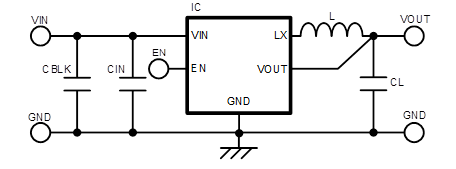
- What is a voltage detector with separate sense terminals?
-
Sense (VSEN) terminal separation function
For a general voltage detector, the power supply of voltage monitoring terminal (sense terminal) is common to that of IC. A product that separates this voltage monitoring terminal (sense terminal) and power supply terminal is called sense (VSEN) terminal separation function or sense (VSEN) terminal separation product.
Separation of power supply terminal and voltage monitoring terminal (sense terminal) has a merit different from general voltage detector.
General voltage detector 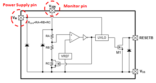
Sense terminal separation function How to utilize the sense terminal separation function
1. The voltage of high-voltage line can be monitored with resistance divider
There are not so many voltage detectors that can directly monitor 12 V line or 24 V line.
When monitoring such high voltage, a method for indirectly monitoring the high voltage by monitoring the voltage dividing the resistance of high voltage is used.
In this method for monitoring voltage after dividing resistance, a general voltage detector whose monitoring terminal and power supply terminal are common causes fluctuation of power supply terminal voltage due to current consumption used for operation of IC, so malfunction may occur.
With a product for which sense terminal is separated, monitoring terminal and power supply terminal are separated. Thus, even if voltage dividing resistance is input to the monitoring terminal, IC does not malfunction and the high voltage can be safely monitored.
An example of monitoring of high-voltage line using a product for which sense terminal is separated is shown below.
In this example, the monitoring voltage of high voltage is divided by resistances R1 and R2 and input to the voltage monitoring terminal (VSEN terminal) of voltage detector. With this, high voltage is not applied to the voltage detector and general-purpose low-voltage voltage detector can be used.
Detect voltage = "detect voltage of voltage detector" x (R1 + R2) / R2
2.A detection signal can be kept even if the sense voltage is 0 V
With a general voltage detector whose monitoring terminal and power supply terminal are common, if the voltage of line to be monitored drops below the IC's operating voltage, the IC's internal circuit cannot normally operate. Thus, a correct detection signal cannot be output when the monitoring voltage is low.
With a product for which sense terminal is separated, if the operating voltage is supplied to the power supply terminal, correct detection signal can be output even if the voltage of sense terminal decreases to 0 V.
- What is backflow prevention function? What is complete backflow prevention function?
-
The backflow prevention function of load switch IC is a function that prevents backflow of current to input side when the voltage on output side becomes higher than input voltage. It is sometimes mounted on voltage regulator or charger IC, etc. in addition to load switch IC.
Case example that requires the backflow prevention function
1.Preventing the backflow to input wide when voltage higher than input voltage is applied to the output side for Vout "OR" connection.
2.Preventing the backflow from capacitor or power storage device that is connected to output side to input side.
3.Preventing energization of output voltage to input side by cutting off input side and output side when external voltage is applied to output side and the power storage device is connected to output side.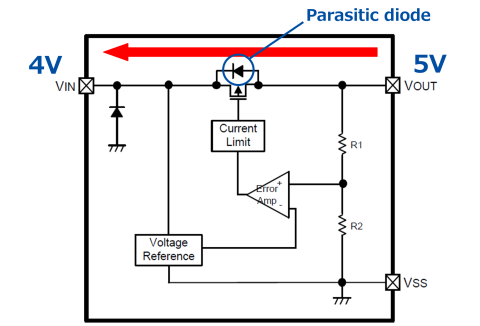
General voltage regulator 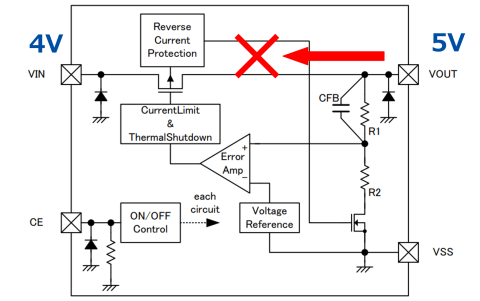
Voltage regulator equipped with backflow prevention function Cautions on backflow prevention function: Backflow may occur even if backflow prevention function is mounted
Although the backflow prevention function seems to prevent backflow from the output side to the input side under any conditions, the current may backflow from output side to input side depending on control system or usage.
For this reason, it is necessary to select a product equipped with appropriate backflow prevention function based on the control system and characteristics of backflow prevention function.
The following explains types and usage of backflow prevention functions.Types of backflow prevention function: backflow prevention function and complete backflow prevention function
The backflow prevention function is roughly classified into two types.
(1) Backflow prevention function
The backflow prevention function is adopted for general load switch IC, etc.
Only when the switch part of load switch IC is turned OFF, the backflow prevention function surely operates.With this type of backflow prevention function, whether there is backflow is judged by input voltage becoming lower than output voltage by more than a certain level.
If the input capacity is small or there is no current sinking from input side, the input voltage rises up to output voltage due to backflow current to input side. For this reason, the dropout voltage with which the backflow prevention function operates cannot be ensured and the phenomenon that the backflow prevention function does not work occurs.As an advantage of this judgment method, when the load switch is turned ON, FET at the switch part can be always fully turned ON and the on-resistance can be reduced.
If the load switch is turned OFF, the input voltage becomes lower than output voltage by more than a certain level before the backflow current flows, so the backflow can be prevented.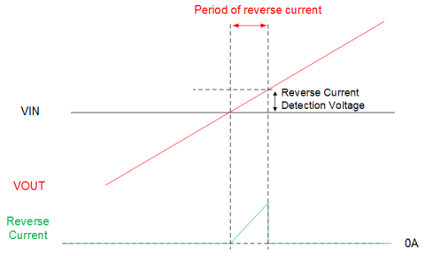
Behavior when VIN<VOUT @ load switch ON 
Behavior when VIN<VOUT @ load switch OFF (2) Complete backflow prevention function
With this function, the backflow prevention function operates regardless of when the switch part of load switch IC is turned ON and OFF.With this type of backflow prevention function, the backflow prevention function operates when the output voltage becomes slightly lower than the input voltage.
In this judgment method, the backflow can be prevented even if the switch part of load switch IC is turned ON.
However, when the load switch is turned ON, it is necessary to keep dropout voltage above a certain level in order to prevent the backflow prevention function from malfunctioning. For this reason, voltage drop and conduction loss tend to increase compared to general backflow prevention function.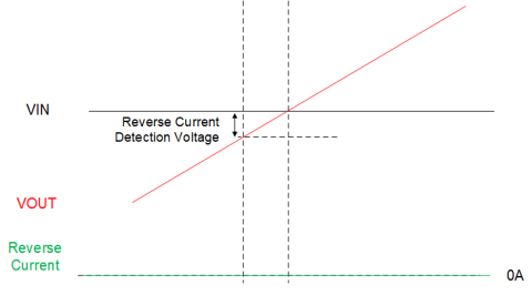
Behavior when VIN<VOUT @ load switch ON - What is chip enable (CE function) and enable function (EN function)?
-
The chip enable function (CE function) and enable function (EN function) are functions that stop all IC operations or part of its functions.
When the IC and part of its functions are operating, it is called to be enabled.
Conversely, when the operation of the IC and part of its functions is stopped, it is called to be disabled.
Generally, in the disabled state where the IC and part of its functions are stopped, output stops and the quiescent current is reduced.
The detailed operation differs depending on the IC, so check the specifications of the IC to be used.
- What is CL discharge (discharge function)?
-
CL discharge (discharge function) is a function that rapidly discharges to capacitance charge connected to the output line during standby. TOREX these are called the CL discharge and CL discharge function, and they are also called by other names, such as discharge function and auto discharge function.
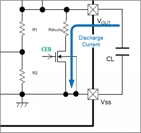
Without a CL discharge function, it is now possible to draw out the output capacitance load during standby, which causes the output voltage to gradually decrease. If the output voltage gradually decreases, it could cause downstream devices to malfunction.
In addition, a power-down sequence may be required by FPGA and other devices. In this case, a CL discharge function is used to quickly power down the output voltage when the power supply sequence is satisfied, so the product must be designed to follow the power-down sequence.
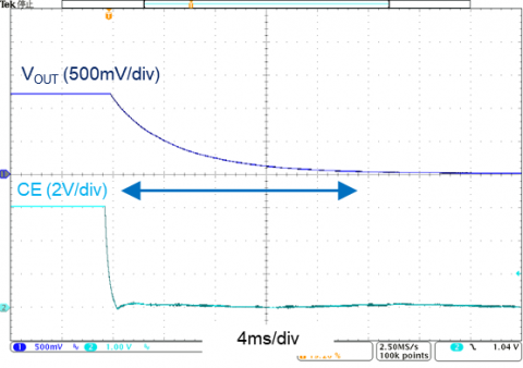
Without CL discharge: XC6221A 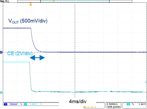
With CL discharge: XC6221B In addition, in some applications the CL discharge function is a demerit.
For applications where an external voltage is applied from the DC/DC or LDO output side using an OR connection, the CL discharge function activates to allow the current to be continuously drawn from the output side.Caution is required because this not only uses the extra quiescent current from the external power supply but could also cause characteristic degradation to occur in the internal elements that conduct the CL discharge.
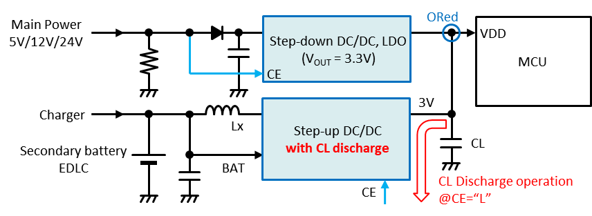
Example where the CL discharge function has a negative impact when OR connected - What is continuous mode (CCM) and discontinuous mode (DCM)
-
Continuous Current Mode (CCM) and Discontinuous Current Mode (DCM) are the names of operation modes of switching power supplies, such as DC/DC and AC/DC.
The CCM and DCM are divided by the flow direction of the coil current. The difference in these operation modes causes a difference in the output voltage stability (transfer function model), so it is important to understand switching power supply control and stability.
The definitions for CCM and DCM are as follows.
Continuous Current Mode (CCM) The coil current is always flowing.
(There is no High Side/Low Side driver FET’s OFF/OFF period.)Discontinuous Current Mode (DCM) There are times when the coil current is not flowing.
(There are High Side/Low Side driver FET’s OFF/OFF period.)Step-down DC/DC CCM
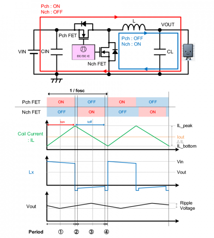
Step-down DC/DC DCM
Generally, DCM is used under light load conditions and then changed to CCM when the output current becomes large. The output current at which the change from CCM to DCM occurs differs for each product and depends on the power supply specifications, inductance, IC control method, etc.
In addition, products that employ forced PWM control even during PWM control operate in CCM without changing to DCM even during light loads.
Condition: Vin=5V, Vout=3.3V/0mA
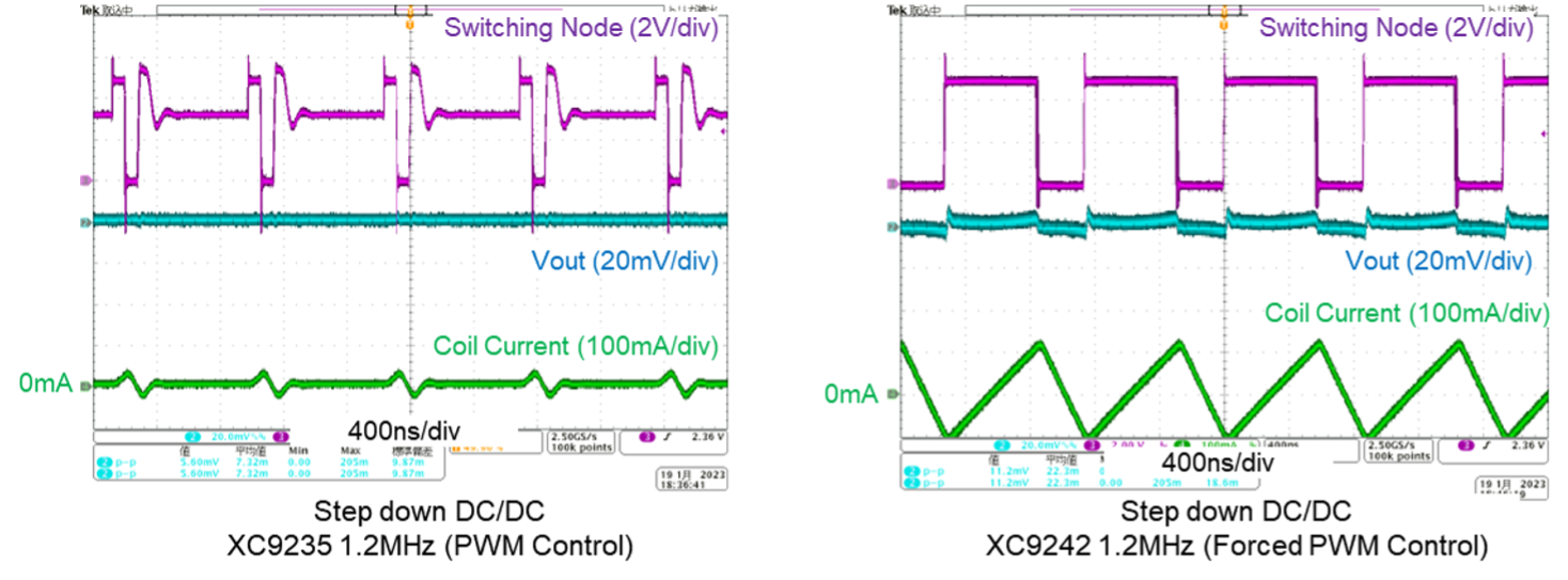
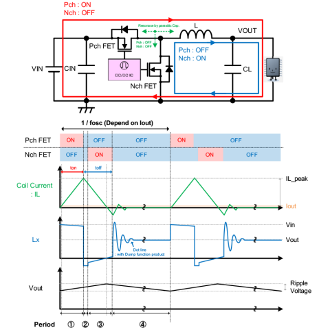
- What is forced PWM mode?
-
In addition to PWM control that prevents reverse flow of the coil current, PWM control that allows reverse flow of the coil current is called forced PWM control.
Condition : Vin=5V, Vout=3.3V/0mA
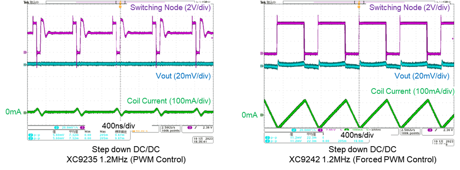
Unlike PWM control, pulse skip does not occur with forced PWM control even at light load conditions and it is easy to take noise countermeasures.
The characteristics of PMW control and forced PWM control are as follows.
PWM Control
This becomes DCM in light load states, and the duty increases as the output current increases.
In the light load state, the ON duty required to maintain the output voltage becomes very small and may become even lower than the minimum duty that can be controlled by the IC.
Under these conditions, the oscillation frequency cannot be maintained and a pulse skip that lowers the oscillation frequency occurs.
In addition, switching node ringing occurs in DCM. Switching node ringing is a cause of output voltage noise interference and radiation noise.
Forced PWM Control
With forced PWM control, it comes CCM even at light loads to reverse the coil current, so the duty is fixed from light loads to heavy loads.
Unlike regular PWM control, the duty does not become small during light loads, so a pulse skip does not occur during light loads.
Further, it does not become DCM, so switching node ringing does not occur and thus ringing is not a cause of noise.
A disadvantage is that the efficiency at light loads is lower than that of regular PWM control.
Further, with forced PWM control, the coil current must be reversed, so forced PWM control with an asynchronous rectifier type DC/DC that requires and externally attached diode cannot be conducted.
- What is ideal diode? What is the difference from discrete?
-
The diode whose forward voltage is 0 equipped with characteristics of passing current in only one direction is called ideal diode.
An IC (integrated circuit) that reproduces the characteristics of this ideal diode is called ideal diode IC. As the ideal diode has no forward voltage drop or current leakage, it has no forward voltage drop, loss, or current leakage that have occurred in discrete diode.
With an actual ideal diode IC, it is possible to completely eliminate forward voltage or current leakage because there are on-resistance and current leakage of FET in IC, however, forward voltage drop and power loss can be considerably reduced compared to diode.
Advantages / disadvantages of ideal diode IC
The ideal diode IC has various advantages compared to discrete diode.
Advantages
- Low loss due to such a small VF & low current leakage
(XC8110/XC8111: VF = 20 mV, discrete SBD: VF = 0.3 to 0.4 V) - As VF is small, output voltage fluctuation is small and it contributes to stable operation of system
- Equipped with various built-in protection functions
- Small PKG
Disadvantages
- Maximum output current and output voltage are restricted
- Number of products is small / less compatible compared to discrete diode
- Low loss due to such a small VF & low current leakage
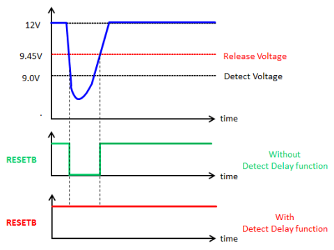
- What is the detect delay of a voltage detector?
-
Detection delay function
The detection delay function of voltage detector is a function that does not output a detection signal immediately after the monitoring voltage reaches the detect voltage, but outputs it after a certain period of time has passed.
This delay time is called detect delay time. There are few voltage detectors equipped with detection delay function. For the voltage detector equipped with this function, the delay time can be externally adjusted using an external capacitor.
The voltage of monitoring line may instantaneously drop at startup of power supply or due to inrush current when the motor operates. The output of wrong detection signal is prevented by using the detection delay function when the voltage detector unintentionally outputs a detection signal due to this instantaneous drop of power supply voltage.
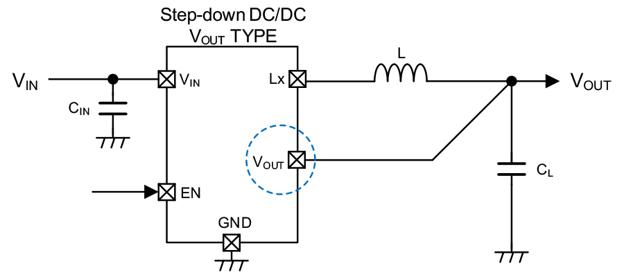
- What is the difference between a DCDC converter and a controller?
-
A DC/DC with a built-in driver FET is called a DC/DC converter.
Conversely, a DC/DC without a built-in driver FET that controls an externally attached FET is called a DC/DC controller.
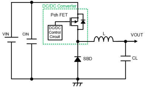
Step-down DC/DC converter 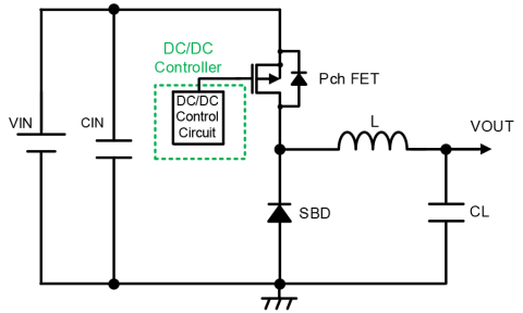
Step-down DC/DC controller When a power supply is configured with a DC/DC converter, it has few externally connected components, which reduces the mounted surface area. However, the driver FET built-in the IC, which is a heat source, and the junction temperature to increase due to power dissipation caused by the driver FET. Therefore, great care with the thermal design is required to ensure the junction temperature stays within the operation range.
A DC/DC controller can be used to build optimum circuits fitting a variety of power supply specifications by selecting the driver FET. However, compared to a DC/DC converter, there are more externally attached components, which increases the mounted surface area. In addition, since increasing the number of components also increases the mounted surface area, the expertise for creating a low-noise design and selecting the optimum peripheral components is required.
DC/DC converter DC/DC controller Number of components/Space saving Good Normal Design difficulty Good Bad Design freedom Normal Good Thermal design Bad Good - What is the oscillation frequency of a switching power supply?
-
The frequency of switching of the switching power supply, such as DC/DC or AC/DC, is called the oscillation frequency.
Generally, the IC shows the switching frequency when switching is performed in a loaded state.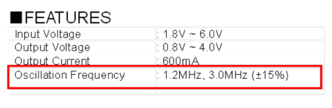
Generally, if the oscillation frequency is high, there are the advantages of component miniaturization and fast response speed, but the disadvantages are the efficiency decreases or the EMI noise increases. For this reason, the optimum oscillation frequency must be selected to match the application and purpose.
Item Effect of High Frequency Oscillation Frequency Efficiency Efficiency declines Component size/mounted surface area Miniaturization Component cost Inexpensive Transient response characteristic Improved responsiveness Ripple voltage Dependent on peripheral components/constant Noise EMI noise worsens In addition, for PFM control and PFM/PWM control, the switching frequency during light loads becomes lower than the oscillation frequency, so care needs to be taken when implementing noise countermeasures.
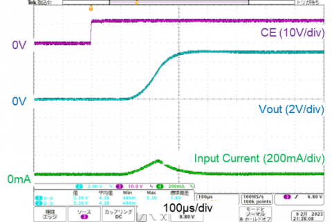
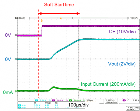
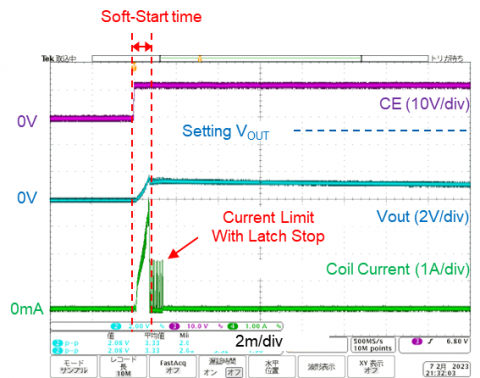
- What is the soft start function and what is the difference from the inrush current prevention function
-
A soft-start function is a function that controls the time from when an IC enters the startup start state until the output voltage reaches the set voltage. When the device contains a soft-start function, the output rise time is constant regardless of the output capacity.
A similar function is the inrush current prevention function. The inrush current prevention function only suppresses the inrush current without controlling the startup time.
Voltage regulator startup waveform
(a) Without soft-start XC6216 @VIN=12V, VOUT=5V
Output capacity: 1μF 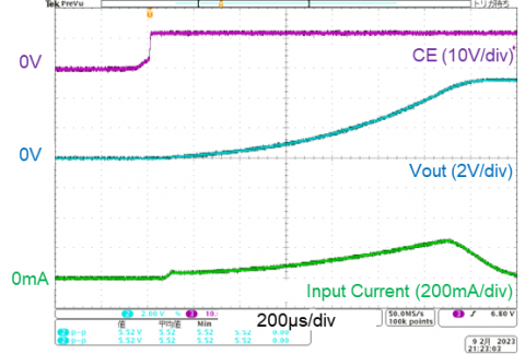
Output capacity: 1μF + 33μF (b) With soft-start XC6702 @VIN=12V, VOUT=5V
Output capacity: 1μF 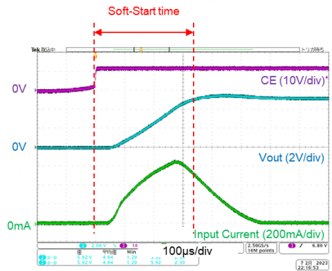
Output capacity: 1μF + 33μF Having a soft-start function has the following advantages.
(a) Suppresses inrush currents and input voltage decreases
(b) Controls the output voltage rise time and slew rate(a) Suppresses inrush currents and input voltage decreases
ICs without a soft-start function are generally used in products where the output voltage slew rate during startup is not controlled. In this case, the IC supplies current to the output side until the output voltage reaches the set output voltage, so an excessive inrush current is generated.
When an excessive inrush current is generated, the impedance on the input side reduces the input voltage. If this reduction in input voltage is large, it could an IC startup failure, system reset, etc.
Voltage regulator startup waveform : VIN=4V, VOUT=3V, CL=1μF, RL=20mA/3.0V
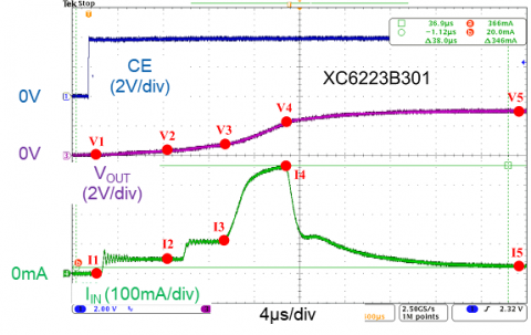
Without inrush current prevention function XC6223B301 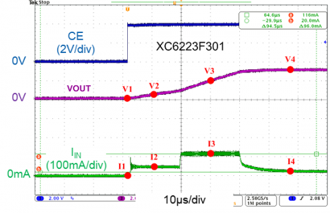
With inrush current prevention function: XC6223F301 (b) Controls the output voltage rise time and slew rate
The soft-start function controls the time from when an IC enters the startup start state until the output voltage reaches the set voltage, so it can be used to adjust the output voltage rise time and slew rate for the startup sequence of downstream devices, etc.
Some products have a fixed soft-start function inside the IC but depending on the product, an externally connected component, etc., can be used to adjust the soft-start time.
Products that can adjust the soft-start time can adjust the output voltage slew rate and reduce the inrush current when a high-capacity capacitor is connected to the output.
When a high-capacity capacitor is connected to the output, the flow of excessive inrush current activates the protective function of the power supply IC, which can cause startup to fail, so generally, this startup failure is prevented by adjusting the soft-start time.
Startup waveform: XC9271 500kHz : VIN=12V/VOUT=5V, CL=22μF x2 + 330μF x 3
Startup failure @soft-start time = 1.3ms 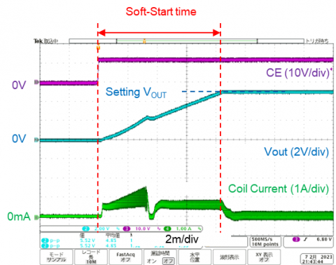
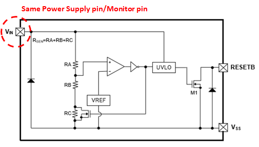
Normal startup @soft-start time = 9ms - What is The Under Voltage Lock Out (UVLO)?
-
The Under Voltage Lock Out (UVLO) function stops the internal circuits to prevent the IC from malfunctioning when the IC power supply is low.
The purpose of this product is not to stop the IC from malfunctioning, but rather is to suppress the quiescent current when the battery voltage drops, so there are also products with a built-in UVLO function.
Generally, for a switching power supply, like DC/DC, when the battery voltage drops causing the UVLO to activate, the switching operation stops. When the power supply voltage subsequently increases, the UVLO function is released, and the switching operation starts.
The detailed behavior differs depending on the product, so the data sheet of each product must be checked.
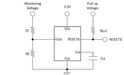
- What is the voltage detector manual reset function?
-
Manual reset function
The manual reset function of voltage detector is a function for forcibly outputting a reset signal (detection signal) even when the monitoring voltage cannot be detected.
The voltage detector is equipped with manual reset terminal. It forcibly outputs a detection signal by inputting an external signal.“Forcible reset button” that is frequently prepared for electronic devices uses this function.
This function is sometimes used for evaluation of test production or debugging, etc. in addition to forcible reset of equipment by end user.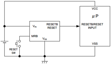
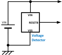
Example of circuit 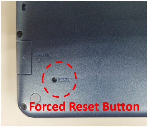
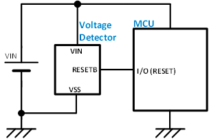
Example of use - What is thermal shutdown/overheat protection?
-
Thermal shutdown is a function that prevents the IC from malfunctioning, suffering characteristic degradation, or being damaged when the IC junction temperature becomes excessively hot.
In the case of general voltage regulators and DC/DC, when the thermal shutdown function activates, the current supply to the output side is stopped, and output turns off.
When the current supply to the output side stops, self-heating stops, which decreases the junction temperature.
For ICs with a built-in self-reset type thermal shutdown function, when the junction temperature decreases to the thermal shutdown reset temperature, the IC restarts.
When the excessive load continues after restarting, the thermal shutdown activates again, and it will behave by repeatedly detection and reset.
DC/DC converter (XC6702): Thermal shutdown detection ⇔ Reset state
(Condition: Vin=11.8V, Vout=1.8V)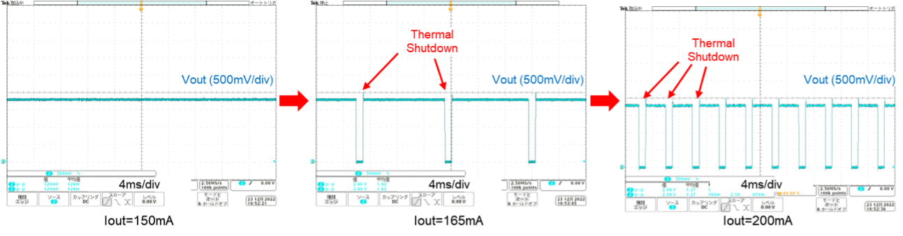
There are also products with a similar function where the charger IC monitors the battery temperature and performs optimum charging control based on the battery temperature state.
- What is voltage detector? How use it?
-
The voltage detector is an IC that monitors the voltage of power supply line to output a detected signal when the voltage falls below or exceeds the setting voltage. The voltage detector is also called VD (abbreviation of voltage detector), reset IC, or supervisor, etc.
The basic relationship between input (monitoring voltage) and output of voltage detector is shown below.
Monitoring voltage Output Release voltage or more
(detect voltage + hysteresis)“H” Detect voltage or less “L” ※Item that outputs "L" at detection (active "L") Use application of voltage detector
1.Monitoring of battery / power supply voltage
The voltage detector monitors the power supply line. If the voltage of power supply line becomes abnormal, a signal is output to the following device. Transmitting the abnormal status to the following device judges the abnormal status or stops the operation of the system.
The voltage detector is also used for monitoring the voltage of battery. Detection of battery voltage drop by voltage detector is used for stopping the operation of system or display of voltage drop status, etc.
2.Reset of MCU / Power On Reset (POR)
For an MCU, operating voltage range is set.
The voltage detector monitors MCU's power supply line. If the voltage of power supply line becomes operating voltage or less, a reset signal is output to stop the MCU. The voltage detector is also utilized to operate the MCU after making sure the power supply line is turned ON.
3.Power supply sequence control
Some MCUs and modules require multiple power supplies such as main power supply and core power supply. For some devices, rise-up / rise-down sequence of each power supply is specified.
It is possible to monitor the power supply line using a voltage detector to start up / fall down the next power supply after rise-up / rise-down of a power supply line.
A power supply sequence can be easily created using this function.
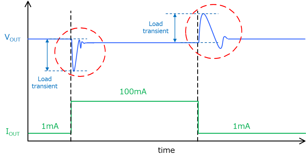
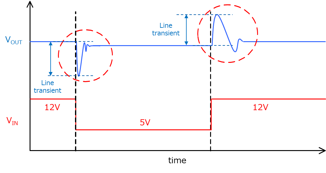
- What kind of characteristics are the load-transient response and line-transient response characteristic?
-
The load-transient response characteristic and the line-transient response characteristic are characteristics that show the amount of output voltage change and responsiveness of the DC/DC and voltage regulator when the output current or the input voltage suddenly change.
Load-transient response characteristic
This shows how much the output voltage changes and how long takes it to converge when the output current suddenly changes.
The output voltage change amount is affected by the IC control method, the output current conditions, and the output capacity, etc.For the voltage regulator, high-speed type voltage regulators have better load-transient response characteristics, but the quiescent current becomes large.
For DC/DC, the control method causes a large change in the load-transient response characteristic, so a product that uses a control method that allows a fast transient response must be selected.
In addition, using the load transient change, it is possible to determine the product stability from the output voltage response wavelength.
Line-transient response characteristic
This shows how much the output voltage changes and how long it takes it to converge when the input voltage suddenly changes.
The line-transient response characteristic is also affected by the IC control method, the input voltage conditions, and the output capacity, etc., the same as is the load-transient response characteristic.Generally, products with a good load-transient response characteristic tend to also have a good line-transient response characteristic.
Automotive Products
- Have you received IATF16949 certification?
-
As a fabless manufacturer, Torex Semiconductor cannot obtain IATF16949 certification. In 2019, we have been registered as a remote support department of the group company's IATF16949 certified factory.▶ Initiatives of IATF16949
Aiso, we are implementing management using the core tools (SPC, MSA) required by IATF16949, and are also offering PPAP documents in response to customer requests. - How are you supporting automotive products?
-
We established the "Kansai Technology Center" in April of 2016 as a central base for expanding our automotive business.
This centralizes the product design, mass production technology, and quality assurance functions that were previously dispersed in various regions, enabling us to offer a comprehensive response capability. - How does Torex define an automotive product?
-
On the release of an automotive electronics product, the AEC certifies the product based on AEC-Q100.
We also implement mass production testing, traceability, and other management procedures that differ from mass production products. - What about quality and environmental measures?
-
We have received ISO9001 and ISO14001 certification. We also meet EU RoHS/REACH requirements and are halogen and antimony free.
- What is AEC-Q100?
-
AEC-Q100 is a standard of the AEC which prescribes a variety of reliability tests for integrated circuits (ICs).